


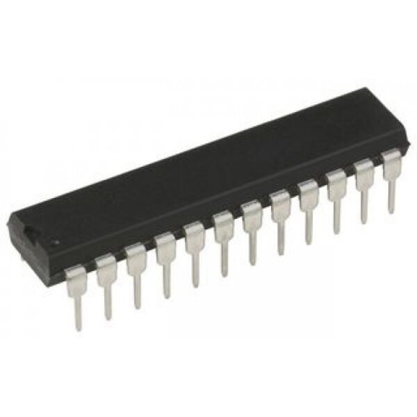
CD4013 Dual D Type Flip-Flop IC DIP-14 Package
Original price was: ₹15.00.₹11.00Current price is: ₹11.00.
The CD4013 device consists of two identical, independent data-type flip-flops. Each flip-flop has independent data, set, reset, and clock inputs and Q and Q outputs. These devices can be used for shift register applications, and, by connecting Q output to the data input, for counter and toggle applications. The logic level present at the D input is transferred to the Q output during the positive-going transition of the clock pulse. Setting or resetting is independent of the clock and is accomplished by a high level on the set or reset line, respectively.
The CD4013 types are supplied in 14-pin dual-in-line plastic packages (E suffix), 14-pin small-outline packages (M, MT, M96, and NSR suffixes), and 14-pin thin shrink small-outline packages (PW and PWR suffixes).
Features:-
- Asynchronous Set-Reset Capability
- Static Flip-Flop Operation
- Medium-Speed Operation: 16 MHz (Typical) Clock Toggle Rate at 10-V Supply
- Standardized Symmetrical Output Characteristics
- Maximum Input Current Of 1-µA at 18 V Over Full Package Temperature Range:
- 100 nA at 18 V and 25°C
- Noise Margin (Over Full Package Temperature Range):
- 1 V at VDD = 5 V
- 2 V at VDD = 10 V
- 2.5 V at VDD = 15 V
Detailed Specifications:-
| Parameters | Specifications |
| Part number | CD4013B |
| Technology Family | CD4000 |
| Input type | Standard CMOS |
| Output type | Push-Pull |
| VCC (Min) (V) | 3 |
| VCC (Max) (V) | 18 |
| Channels (#) | 2 |
| Clock Frequency (Max) (MHz) | 24 |
| ICC (uA) | 600 |
| IOL (Max) (mA) | 6.8 |
| IOH (Max) (mA) | -6.8 |
| Features | Balanced outputs, Standard speed (tpd > 50ns), Positive input clamp diode |
| Rating | See Data Sheet |
| Package Group | PDIP|14 |
* Product Images are shown for illustrative purposes only and may differ from actual product.


Reviews
Clear filtersThere are no reviews yet.